-
(b.) - ?1938 September 17
Bio/Description
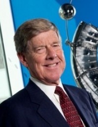
An Anglo-Australian electrical engineer, he was born in Calcutta, India and educated at Geelong Grammar School in 1948. He attended Melbourne University in Australia receiving his B.Sc. degree in Physics in 1959. In 1962, he obtained his B.A. degree in Electrical Sciences from the University of Cambridge in England, after arriving initially as a choral scholar. He then received his Ph.D. degree from the University of Cambridge in 1965; his thesis was titled, ?Selective ion beam etching in the scanning electron microscope?. A pioneer of nanotechnology, while in the Engineering Department of the University of Cambridge, he began his research career in 1961 working with Professor Oatley, and later with Dr. William C Nixon, on the in situ study of surfaces undergoing ion etching in the scanning electron microscope (SEM). The microscope he used had originally been built by Oatley and had then been modified Garry Stewart who had also added an ion source that focused ions onto the sample surface. During his Ph.D. he rebuilt the SEM fitting a magnetic final lens in place of the original electrostatic lens thereby improving the microscope's resolution to about 10 nm, and after examining ion etched surfaces, used the microscope's electron beam for the first time to write patterns, subsequently using ion etching to transfer these patterns into gold, tungsten and silicon structures as small as 40 nm. These were the first man-made nanostructures in materials suitable for microelectronic circuits opening up the possibility for the extreme miniaturization of electronic circuits that was to occur in the decades to come. He then worked in the research and development laboratories of IBM in the United States for 19 years before returning to Cambridge in 1984 to become Professor of Electrical Engineering (1984?96) and Fellow of Trinity College, Cambridge (1985?90). He set up a nanofabrication laboratory to extend the technology of miniaturization to the atomic scale by developing some of the novel fabrication methods that he had discovered at IBM. He modified a 400 KV transmission electron microscope (JEOL 4000EX) so that it operated in a scanning mode and produced a minimum beam size of about 0.3 nm. He used this system working in collaboration with researchers at the IMEC microelectronics research laboratory in Leuven, Belgium, to build some of the smallest and fastest field effect transistors that had ever been built. He subsequently became Master of Churchill College, Cambridge (1990?96) and Head of the Cambridge University Engineering Department (1993?96). He was Vice-Chancellor of Cambridge University, 1996?2003. In 1997 he was invited to deliver the MacMillan Memorial Lecture to the Institution of Engineers and Shipbuilders in Scotland. He chose the subject ?The Role and Education of the Creative Engineer?. In 1997 he became a non-executive Director of Vodafone, a British multinational telecommunications company headquartered in London and with its registered office in Newbury, Berkshire. He was knighted in 1998 and created a life peer in 2004, as Baron Broers of Cambridge in the County of Cambridgeshire. He was Chairman of the Science and Technology Committee of the House of Lords from 2004 to 2007 and was President of the Royal Academy of Engineering from 2001 to 2006. In September 2008, he took over from Sir David Cooksey as Chairman of the Board of Directors at the Diamond Light Source, the United Kingdom's largest new scientific facility for 45 years. In 2009 he became Chairman of Bio Nano Consulting and in 2010 he was named Chairman of the Technology Strategy Board Knowledge Transfer Network for Transport. In 2012 he became Chairman of the Judging Panel of the Queen Elizabeth Prize for Engineering. He has received more than twenty honorary degrees and fellowships from universities, colleges, and academic and professional institutions. He is a Foreign Member of the U.S. National Academy of Engineering, the Chinese Academy of Engineering, the Australian Academy of Technological Sciences and Engineering, and the American Philosophical Society.
-
Date of Birth:
1938 September 17 -
Noted For:
Pioneer of nanotechnology developing the first man-made nanostructures in materials suitable for microelectronic circuits opening up the possibility for the extreme miniaturization of electronic circuits -
Category of Achievement:
-
More Info:


